
The most efficient storage device: DNA chip and perovskite
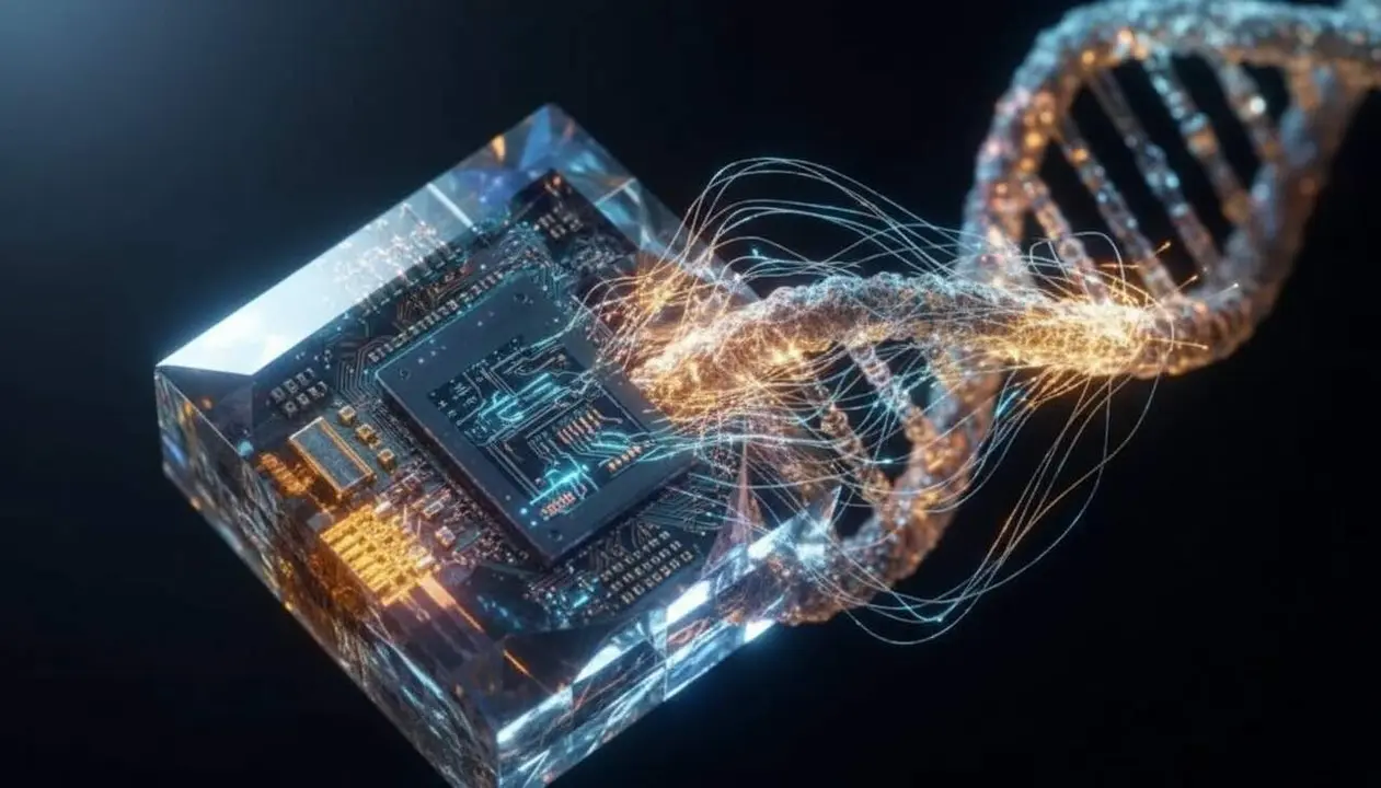

The original article comes from Penn State University and has been published in the journal Advanced Functional Materials. The device, called a biohybrid memristor, merges the conductive properties of synthetic DNA doped with silver nanoparticles and the electrical regulation of crystalline perovskite.
The technical key is that synthetic DNA, with a storage capacity of about 215 million gigabytes per gram, has become a stable electrical conductor thanks to doping with silver, allowing the perovskite to regulate the charge flow. This makes the device consume less than 0.1 volts and withstand up to 121 °C, maintaining stability for weeks.
How does the device work and why is it revolutionary?
What is a memristor and how does it mimic the human brain?
A memristor (a combination of memory and resistor) remembers the electrical state it was left in after current has passed, even if the power source is turned off. This eliminates the need to maintain constant power, unlike conventional RAM.
Moreover, this device processes data where it stores it, just like a neuron, avoiding the transfer of information between memory and processor. This solves the energy bottleneck known as the Von Neumann bottleneck, critical in artificial intelligence.
What benefits does it bring to artificial intelligence?
Practically, the biohybrid memristor could reduce energy consumption in data centers and AI systems by more than 99%, which currently require megawatts for large models like ChatGPT. This represents a leap towards sustainable and compact AI.
How to activate and integrate this technology?
What steps are followed for its commercialization?
Although the device is in the experimental phase, scientists indicate that the process to bring it to mass production will be long, with years of industrial scaling, integration with existing architectures, and reliability testing.
The patent, registered in April 2026, is the first step towards future adoption that could take nearly a decade.
How is it verified that a system can incorporate this technology?
- Device stability at room temperature for weeks exists.
- Operation at ultra-low voltages (less than 0.1 V) is consistent.
- Integrity maintenance at high temperatures (up to 121 °C).
- Storage capacity comparable to that of a gram of synthetic DNA (more than 200 million gigabytes).
- Local information processing without the need for external transfers.
| Platform / Version | Added | Patch Available |
|---|---|---|
| Penn State Biohybrid Memristor | Yes | In industrial scaling process |
| Conventional Flash Memory | No | Regular updates |
| Conventional RAM | No | Regular updates |
Tips for prevention and maintenance in storage systems
Keeping systems updated and reviewing access permissions is basic to ensure security. Additionally, activating multi-factor authentication (2FA) and making frequent backups are key to avoiding data loss.
It is necessary to watch for signs such as unusual slowness, repeated errors, or system crashes, which may indicate problems with memory or processing. In such cases, consulting an expert in hardware or advanced memory systems is advised.
The reality is that this technological advance opens the door to more sustainable and powerful new devices, but it also demands gradual and vigilant adaptation in the industry and end users.